by Doug McInnis
 Imagine an object that’s 1/50,000th the width of a human hair.
That’s the scale at which science works today to turn out faster computers.
And some of the nation’s leading edge entrepreneurs are betting their futures that this science—nanotechnology will pay off big.
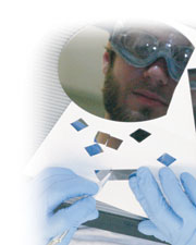
One of these is Norman Schumaker ’63, whose startup company, Molecular Imprints, aims to bring down the costs of making the silicon chips that form the brains of your computer, Palm, iPod, and the instruments your surgeon uses.
Schumaker visited Wabash in April to bring faculty and students—particularly Professor Lon Porter’s nanotechnology class—up to speed on his work and developments in the field.
The Challenge
It costs up to $4 billion to build a new plant to turn silicon chips into immensely powerful integrated circuits. About $1 billion of that pays for lithography equipment to imprint tiny patterns on the surface of silicon chips. These nanoscale paths carry the electrons that do the heavy lifting in information processing.
Schumaker’s company hopes to greatly simplify the imprinting process, so that making chips is about as simple as stamping out automobile bumpers or bottle caps in a factory. By doing so, Schumaker said, “We can cut lithography costs in new chip factories from about $1 billion to $100 million.”
Molecular Imprints builds tools that make the miniscule features and structures on the surface of silicon chip-surfaces. They’ve taken a leaf from old-fashioned industrial production methods, where machine tools such as the stamping press rapidly knock out the same part over and over.
“On a stamping machine, once you have a master mold, you can make millions of replicas,” Shumaker said
|
"At a small company, | |
This master template with the desired pattern is created from fused silica and attached to the special tool built by Molecular Imprints. The pattern is reproduced on silicon at high speed and incredible accuracy. Each pathway on the pattern can be as small as 20 nanometers wide. (A nanometer is one-billionth of a meter.)
Schumaker compared the new process to Gutenberg’s invention of the printing press, which eventually led to mass-produced, less expensive books, making texts available to the populace.
“We’re going to do the same thing for chips,” predicted Schumaker, who serves as Molecular Imprints President and CEO.
The imprinting process used by Schumaker’s company was developed at the University of Texas at Austin, not far from the Molecular Imprints headquarters. Schumaker’s firm paid the university for the exclusive rights to turn that technology into a practical product that could be sold commercially. The first prototype machines will soon be shipped for testing. Buyers include a Korean research institute, a West Coast semi-conductor manufacturer, and Motorola. Each machine costs $1.5 to $2 million. Meanwhile, employment at Molecular Imprints has reached 60 people.
“I read everything”
Schumaker grew up in Michigan City, Indiana, and was the first in his family to attend college. When he arrived at Wabash, he was already well read, having picked up the love of books during a childhood illness in the early 1950s. “I was confined to bed for nine or ten months. There was no TV. When you’re in bed, there’s not much you can do but read. I read everything I could get my hands on—biographies, histories of the Civil War, the history of science.”
Wabash gave Schumaker a very strong scientific education. But the College also led him to a graduate school that would shape his career. “You’re going to MIT,” Professor Ed Haenisch, the College’s famed chemistry department chairman, told Schumaker.
“I didn’t know anything about MIT,” Schumaker said. “He made the decision for reasons that still mystify me. I would not have applied were it not for his urging.”
It turned out to be a good choice. MIT prepared Schumaker for a career in chemistry and paved the way for him to join Bell Labs, the inventive research arm of the-then-giant AT&T Corp. Bell Labs was doing groundbreaking work in lasers, but an antitrust decree broke up AT&T in 1984. Schumaker knew that the downsized company could not sustain Bell Labs at its creative best. He left for an entrepreneurial career at age 44 and founded Emcore, a start-up that helped change the direction of compound semiconductor technology.
Since leaving Bell Labs, Schumaker hasn’t glanced back. “Once you’ve [made the break], you can’t go back to a large organization,” he says. “At a small company, you know the people better. You have the opportunity to determine what gets accomplished. You have the joy and terror of living on the edge.”
Why nanotech at Wabash?
Nobel laureate Richard Feynman’s speech to a gathering of the American Physical Society in 1959 pushed the idea of creating new branches of science based on a nanoscale. The result was a sea-change in scientific thinking that led scientists to believe they might build new devices one molecule at a time.
 | |
|
Greg Fulmer '05 cuts silicon wafers during his nanotechnology research with Professor Porter. |
With money to be made, nanotechnology has become a staple of research at major research universities. It’s found in Wabash classrooms, where nanotech concepts are being introduced throughout the science curriculum. The College also offers a new introductory course on nanotechnology, making Wabash one of only a handful of liberal arts institutions offering a course devoted solely to the subject.
“Nanotech encompasses the fundamentals of biology, chemistry, physics, and mathematics,” says Professor Porter, who taught the College’s first nanotech course this year. “It is a discipline in which the sciences come together, and that’s where the great discoveries are to be made.”
One of today’s great challenges brings computer science and nanotechnology together, Porter explains. The old lithography process used to make integrated circuits is slow and expensive. Having Schumaker, an innovator in the field, available to students was an enriching moment for the class.
“You’ve got to get faster, smaller, and cheaper chips,” says Porter. “So you’ve got to find something that can make the pathways on the chips smaller, and can do it reliably and cheaply. Schumaker’s company can do that, and he was able to tell our students how it’s done.”
Molecular Imprints also illustrates how pure research eventually is incorporated into applied commercial technology, an important lesson for Wabash students in any major.
“As long as there is a continuing flow of ideas, there will be new products and new jobs,” Schumaker said. “If you don’t continue to fund research (both pure and applied) you will get an economic death spiral.”
The rewards for success can be immense, but the path to fame and riches is littered with failed products, bankruptcies, and battered entrepreneurs.
“The highs are really high and the lows are really low,” said Schumaker. At its worst, he said, “You’re going down this steep incline and hoping for dear life that there will be a bottom.
“I call it white-knuckle time. In my previous company, we went from 107 employees to 49 and I was planning to take the company down to 12 people. We had gone nine months without an order.” Then the company notched a $5.5 million sale.
“Every entrepreneur has the same struggles of trying to generate sales and raise money to pay the bills. The biggest struggle is to stay alive long enough to generate the benefits you have envisioned.”